


What Is The Difference Between N Type And P Type Semiconductor: A Detailed Overview
26 June 2026
5 Mins Read
- What Is A Semiconductor?
- What is a P-Type Semiconductor?
- Characteristics Of A P Type Semiconductor
- What is an N-Type Semiconductor?
- Characteristics Of A N-Type Semiconductor
- Difference Between N Type And P Type Semiconductor
- What Are The Applications Of N Type And P Type Semiconductors?
- N Type And P Type Semiconductors: Common Misconceptions
- 1. P-Type Material
- 2. N-Type Material
- 3. Understanding Holes
- The Difference Between N Type And P Type Semiconductors Explained
Semiconductors play an important role in contemporary electronics, being integral components in devices such as:
- Smartphones
- Laptops
- Electric Vehicles
- Advanced Chips
A fundamental aspect of semiconductor technology involves doping, which gives rise to two primary types: p-type and n-type semiconductors.
A clear understanding of these types is essential for anyone interested in electronics, VLSI (Very Large Scale Integration), and semiconductor engineering.
This article provides a comprehensive overview of the difference between n type and p type semiconductors.
What Is A Semiconductor?
A semiconductor is a material that exhibits electrical conductivity between that of a conductor and an insulator.
In its pure form, it is referred to as an intrinsic semiconductor.
One of the most notable examples of this will be silicon.
It possesses only a limited number of free charge carriers at room temperature.
Moreover, to enhance its conductivity for practical applications, engineers employ a process known as doping.
What is a P-Type Semiconductor?
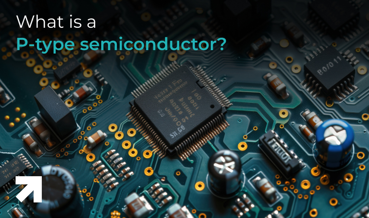
P-type semiconductors are formed by doping a pure semiconductor with trivalent (acceptor) impurities, such as boron, aluminum, or gallium.
The introduction of these impurities results in the following characteristics:
- The dopant atoms have three valence electrons.
- One of the bonds remains incomplete, leading to the formation of a hole.
Holes serve as positive charge carriers and are considered the majority carriers, while electrons become the minority carriers within p-type semiconductors.
This majority carrier phenomenon is important for conduction.
Characteristics Of A P Type Semiconductor
P-type semiconductors have distinct properties that render them essential in various electronic applications.
One of their key features is their lower conductivity, making them ideal for devices that necessitate a controlled flow of electric current.
Unlike N-type semiconductors, P-type materials exhibit a positive charge due to holes.
This creates an overall positive charge in the material.
This characteristic is vital for certain electronic devices as it enables the manipulation of electric current flow.
Furthermore, P-type semiconductors typically demonstrate increased resistance.
Professionals will know that this trait can be beneficial in applications requiring precise control of electric current.
| Examples of P-Type Semiconductors: | Applications of P-Type Semiconductors |
| Silicon doped with boron | Forming PN junctions |
| Silicon doped with aluminum | Serving as the base region of bipolar junction transistors |
| Germanium doped with gallium | Implementing CMOS logic circuits |
What is an N-Type Semiconductor?
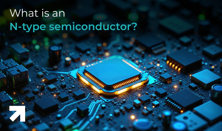
N-type semiconductors are created by doping a pure semiconductor with pentavalent (donor) impurities, such as phosphorus, arsenic, or antimony.
In this case, the impurity atoms have five valence electrons:
- Four of these electrons form covalent bonds with the silicon atoms.
- The fifth electron becomes free and contributes to electrical conduction.
In n-type semiconductors, electrons function as the majority carriers while holes act as the minority carriers.
Because it contains negatively charged electrons, this type of semiconductor is referred to as n-type.
Characteristics Of A N-Type Semiconductor
N-type semiconductors possess several distinctive properties that render them effective for various applications.
One of their primary attributes is high electrical conductivity.
This makes them suitable for components that require efficient electron flow, such as
- Transistors
- Diodes
Moreover, N-type semiconductors are characterized by a negative charge due to the surplus of electrons within their structure.
This negative charge is essential for the operation of numerous electronic devices.
Also, this enables precise control of the electric current.
Furthermore, N-type semiconductors exhibit relatively low resistance.
So, this facilitates the flow of electric current. It also enhances their performance in electronic circuits.
| Examples of N-Type Semiconductors: | Applications of N-Type Semiconductors |
| Silicon doped with phosphorus | The source and drain regions of transistors |
| Silicon doped with arsenic | Integrated circuits |
| Germanium doped with antimony | — |
Difference Between N Type And P Type Semiconductor
| Feature | N-Type Semiconductor | P-Type Semiconductor |
| Doping Element | Pentavalent impurities (e.g., phosphorus, arsenic) | Trivalent impurities (e.g., boron, aluminum) |
| Charge Carriers | Electrons (negative) | Holes (positive) |
| Majority Carriers | Electrons | Holes |
| Minority Carriers | Holes | Electrons |
| Conduction Type | Driven by electron movement | Driven by hole movement |
| Fermi Level Position | Between the donor level and the conduction band | Between the acceptor level and the valence band |
| Electrical Properties | Higher carrier mobility | Lower carrier mobility |
| Energy Band Diagram | Fermi level near the conduction band | Fermi level near the valence band |
| Application | Diodes, transistors, solar cells, ICs | Diodes, transistors, solar cells, ICs |
| Example Materials | Silicon with phosphorus/arsenic | Silicon with boron/aluminum |
| PN Junction Behavior | Electrons move to the P-type region | Holes move to the N-type region |
Also Read: How Does Industrial Innovation Affect Industries?
What Are The Applications Of N Type And P Type Semiconductors?
The unique characteristics of N-type and P-type semiconductors play a vital role in various electronic applications.
N-type semiconductors are particularly valuable in components such as:
- Transistors
- Diodes
- Integrated Circuits
This is where the efficient flow of electrons is essential for optimal performance.
Additionally, their high concentration of free electrons makes them ideal for photovoltaic cells, enabling the efficient conversion of light energy into electrical energy.
Conversely, P-type semiconductors are important in applications such as solar cells, where the movement of holes is important for generating an electric current.
They also play a prominent role in diodes and bipolar junction transistors, which rely on a controlled flow of electric current to function properly.
Together, N-type and P-type semiconductors form the foundation for many critical electronic devices and technologies.
N Type And P Type Semiconductors: Common Misconceptions
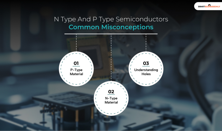
There are several common misconceptions regarding P-type and N-type semiconductor materials that are important to clarify.
Having clarity on these topics is essential for a deeper conceptual understanding of semiconductor physics.
1. P-Type Material
It is often believed that P-type materials are positively charged.
However, this is a misunderstanding, as these materials are fundamentally neutral.
In P-type semiconductors, holes act as the majority carriers, representing the absence of electrons.
2. N-Type Material
Another misconception is that N-type materials consist of negative charges.
This is misleading because while electrons are the majority carriers in N-type semiconductors, that does not imply any net charge; the material remains neutral.
3. Understanding Holes
Some people consider holes to be real particles.
This is incorrect, as holes are defined as the absence of electrons and do not exist as independent entities.
The Difference Between N Type And P Type Semiconductors Explained
If you are new to the technology sector, it is very important that you understand the distinctions between N-type and P-type semiconductors.
Electronic devices depend heavily on the accurate control of electric current. In fact, so does circuits.
Furthermore, this is significantly influenced by the choice of semiconductor materials.
Therefore, you must be able to recognize the unique properties and behaviors of N-type and P-type semiconductors.
Also, this enables engineers and scientists to design and refine electronic components tailored for specific applications.
This expertise is vital for progress in various domains, including:
- Telecommunications
- Renewable Energy
- Computing
Moreover, a deep understanding of these semiconductor types fosters the development of more efficient and innovative electronic devices. Therefore, this drives advancements across technology fields.
Also Check: How To Fix GPS Not Working: Quick Ways To Restore Your Location Services


Related Articles